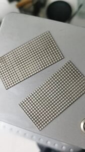
Metallized BeO Ceramic: Properties, Metallization Process and Applications
Metallized BeO ceramic combines the thermal and electrical properties of beryllium oxide (BeO) with an engineered metal layer on selected ceramic surfaces. This combination allows BeO components to be integrated with metal parts through brazing, soldering, electrical connection, or hermetic ceramic-to-metal assembly.
Beryllium oxide is used where high thermal conductivity and electrical insulation are required in the same ceramic component. Metallization extends the functionality of the ceramic by creating a controlled interface for joining and electrical integration.
For RF and microwave electronics, high-power semiconductor packaging, vacuum electronics, and specialized hermetic assemblies, metallized BeO ceramic can provide a useful combination of thermal management, electrical insulation, and package integration.
The appropriate metallization system depends on the BeO grade, component geometry, joining method, electrical requirements, operating temperature, and reliability requirements.
What Is Metallized BeO Ceramic?
Metallized BeO ceramic is a beryllium oxide ceramic component with a controlled metallic layer applied to one or more specified surfaces.
The metallized area may be designed for:
- Brazing to metal components
- Soldering or electrical connection
- Hermetic ceramic-to-metal sealing
- Conductive circuit patterns
- Attachment of pins, housings, or other metallic structures
- Integration into RF and microwave packages
Unlike a simple decorative or protective coating, ceramic metallization is an engineered interface. The metallized layer must provide the required adhesion to the ceramic while also being compatible with the subsequent assembly process.
Depending on the application, the metallization may be applied to a flat surface, edge, internal hole, cylindrical surface, stepped structure, or other customized geometry.
Why Is BeO Used for Metallized Ceramic Components?
The main reason to select BeO is its combination of high thermal conductivity and electrical insulation.
High Thermal Conductivity
BeO can dissipate heat more effectively than conventional alumina ceramics, making it useful for components exposed to high power density.
The actual thermal conductivity depends on BeO grade, density, microstructure, processing conditions, and measurement method. Therefore, material specifications should be evaluated according to the required grade and test conditions rather than relying on a single universal value.
Electrical Insulation
BeO is an electrically insulating ceramic. This allows a component to provide electrical isolation while still transferring heat away from a high-power device.
This combination is particularly useful in applications where conductive metals cannot directly provide the required electrical isolation.
Suitable Dielectric Characteristics
BeO also offers useful dielectric characteristics for selected high-frequency applications. This is one reason it has been used in RF and microwave components where both thermal and electrical performance are important.
Actual dielectric properties should be evaluated at the relevant frequency, temperature, material grade, and measurement conditions.
High-Temperature Capability
BeO maintains its ceramic structure at high temperatures and can be incorporated into assemblies designed for demanding thermal environments.
However, the maximum operating temperature of a finished metallized component depends not only on the ceramic but also on the metallization system, plating, brazing alloy, metal components, and assembly design.
How Is BeO Ceramic Metallized?
The metallization process depends on the required electrical, mechanical, and joining performance.
A typical manufacturing sequence may include:
- BeO Ceramic Preparation
The BeO ceramic is manufactured to the required composition, density, dimensions, surface condition, and geometry.
For customized components, dimensional shrinkage during ceramic sintering must be considered during the manufacturing design.
- Surface Preparation
The ceramic surface is prepared before metallization.
Surface condition, cleanliness, roughness, contamination control, and the geometry of the metallized area can all influence the quality of the final interface.
- Metallization
A suitable metallization system is applied to the specified ceramic surfaces.
Depending on the application, this may include Mo-Mn-based metallization, thick-film systems, thin-film deposition, or other application-specific approaches.
- Firing or Deposition
For fired metallization systems, the metallized ceramic is processed under controlled thermal conditions to develop the required ceramic-metal interface.
For thin-film or other deposition technologies, the process parameters depend on the selected deposition method and required film structure.
- Plating or Surface Finishing
Additional plating may be applied when required for:
- Brazing
- Soldering
- Corrosion resistance
- Electrical contact
- Surface compatibility
- Wire or component attachment
Nickel and gold finishes may be used for selected applications, depending on the assembly requirements.
- Inspection
Finished metallized BeO components may be inspected for:
- Dimensions
- Surface condition
- Metallization coverage
- Metallization integrity
- Adhesion
- Plating quality
- Electrical requirements
- Other customer-defined characteristics
The inspection plan should be established according to the critical characteristics of the component.
Common Metallization Technologies for BeO Ceramic
Different metallization technologies serve different engineering requirements.
| Metallization Method | Typical Purpose | Key Considerations |
| Mo-Mn Metallization | Ceramic-to-metal joining and brazing | Adhesion, firing conditions, plating and brazing compatibility |
| Thick-Film Metallization | Conductive patterns and electrical interfaces | Pattern geometry, conductor properties and firing |
| Thin-Film Metallization | Fine conductive structures and RF applications | Film thickness, pattern resolution and deposition process |
| Customized Metallization | Application-specific assemblies | Geometry, joining process and electrical requirements |
No single metallization system is suitable for every BeO application.
The correct choice depends on the intended joining process, electrical requirements, operating environment, component geometry, and required reliability.
For projects involving detailed metallization process selection, the process should be evaluated together with the ceramic grade and final assembly method.
Mo-Mn Metallization on BeO Ceramic
Mo-Mn metallization is one approach used to create a brazable metalized surface on ceramic.
The basic concept is to form a metallized layer that can subsequently receive plating and provide a suitable surface for brazing to compatible metal components.
For BeO components, the engineering considerations may include:
- Ceramic surface condition
- Metallization composition
- Metallization coverage
- Firing conditions
- Metallization adhesion
- Nickel plating
- Brazing alloy compatibility
- Thermal expansion behavior
- Joint geometry
The exact process parameters should be established and validated for the specific BeO composition, component geometry, metallization system, and joining process.
For a detailed discussion of ceramic metallization methods, see the dedicated Alumina Ceramic Metallization Methods and Mo-Mn Metallization Process resources within the Coraynic technical content cluster.
Applications of Metallized BeO Ceramic
Metallized BeO ceramic is particularly relevant to applications where thermal management, electrical insulation, and metal integration are required simultaneously.
RF and Microwave Packages
BeO has long been associated with high-power RF and microwave applications because of its combination of thermal conductivity, electrical insulation, and useful dielectric characteristics.
Metallization can provide an interface for integrating the ceramic with metal housings, conductors, heat-spreading structures, or other package components.
Typical applications may include:
- RF power packages
- Microwave power components
- High-power amplifier assemblies
- Microwave vacuum devices
- RF feedthroughs
- Hermetic electronic packages
High-Power Semiconductor Packaging
High-power semiconductor devices generate substantial heat during operation.
BeO ceramic can provide electrical isolation while transferring heat from the device toward a heat-spreading or package structure.
Metallized surfaces can then support attachment, brazing, soldering, or electrical integration within the package.
The suitability of BeO should be evaluated against alternatives such as alumina or aluminum nitride according to thermal requirements, electrical characteristics, mechanical design, cost, and manufacturing requirements.
Vacuum Electronic Devices
Metallized BeO can be incorporated into vacuum electronic assemblies where ceramic insulation must be combined with metallic structures.
Potential applications include:
- Vacuum feedthroughs
- Ceramic supports
- Hermetic packages
- RF and microwave vacuum devices
- High-voltage insulating components
For vacuum applications, the metallization and ceramic-metal joint must be compatible with the required hermeticity, thermal conditions, cleaning process, and vacuum environment.
Metallization provides a controlled interface between BeO ceramic and a compatible metal component.
This can enable:
- Brazed assemblies
- Hermetic seals
- Metal housings
- Electrical terminals
- RF feedthroughs
- Customized ceramic-metal components
The final joint performance depends on the complete assembly rather than the ceramic alone.
Metallized BeO Ceramic vs. Bare BeO Ceramic
The main difference is the function of the ceramic surface.
| Feature | Bare BeO Ceramic | Metallized BeO Ceramic |
| Thermal management | Excellent potential | Retained |
| Electrical insulation | Available | Available in non-metallized areas |
| Direct metal joining | Limited | Improved through engineered interface |
| Brazing | Requires suitable joining approach | Metallized surface can provide a brazable interface |
| Electrical connection | Limited | Available on specified metallized areas |
| Hermetic assembly | Requires additional interface design | Suitable for selected ceramic-to-metal sealing designs |
| Package integration | More limited | More options for metal integration |
Metallization therefore should not be viewed simply as adding a conductive layer.
It is a way of modifying selected ceramic surfaces so that the BeO component can perform as part of a larger electrical, mechanical, or hermetic assembly.
Design Considerations for Metallized BeO Components
Successful metallized BeO components should be designed around the complete assembly rather than the ceramic material alone.
BeO Grade and Purity
The selected BeO grade should match the required thermal, electrical, mechanical, and manufacturing characteristics.
Coraynic supports BeO ceramic grades including 99% and 99.5% for different application requirements.
Metallization Pattern
The metallized area can be designed according to the assembly.
Possible configurations include:
- Full-surface metallization
- Selective-area metallization
- Edge metallization
- Internal-hole metallization
- Cylindrical metallization
- Customized patterns
The metallization boundary should be considered together with tolerances, brazing clearance, component alignment, and thermal stresses.
Surface Finish
Nickel, gold, or other specified finishes may be considered depending on the intended brazing, soldering, electrical, or environmental requirements.
The finish should be selected together with the assembly process rather than independently.
Dimensional Tolerance
Ceramic components are subject to dimensional changes during forming and sintering.
For precision components, the final drawing should distinguish between:
- Critical dimensions
- Functional dimensions
- Metallization locations
- Joining surfaces
- Non-critical dimensions
This helps reduce unnecessary manufacturing complexity and improves process consistency.
Thermal Expansion and Joint Design
The BeO ceramic, metallization, brazing alloy, and metal housing may have different coefficients of thermal expansion.
The joint therefore needs to be designed as a system.
Factors to consider include:
- Material combinations
- Joint geometry
- Brazing temperature
- Thermal cycling
- Mechanical constraints
- Component size
- Metallized area
Reliability Considerations
Metallized BeO components may experience thermal, mechanical, electrical, and chemical stresses during manufacturing and service.
Important reliability considerations include:
Metallization Adhesion
The metallized layer must remain securely bonded to the ceramic throughout processing and service.
Poor adhesion can lead to peeling, cracking, or loss of electrical and joining functionality.
Thermal Cycling
Repeated heating and cooling can generate stress at ceramic-metal interfaces because of differences in thermal expansion.
The ceramic, metallization, plating, brazing alloy, and metal structure should therefore be considered together.
Brazing Compatibility
The metallized surface must be compatible with the selected brazing alloy and joining conditions.
Wetting, joint geometry, thermal profile, and surface cleanliness can all affect the final joint.
Surface Cleanliness
Contamination can affect metallization quality, brazing, soldering, electrical performance, and hermeticity.
Cleaning and handling procedures should therefore be defined according to the final application.
Hermeticity
For vacuum or sealed electronic packages, the ceramic-metal interface may need to meet a specified leak-rate requirement.
Hermeticity should be verified using an appropriate inspection method based on the application.
For a deeper discussion of metallized BeO reliability, refer to Coraynic’s dedicated article on Metallized BeO Ceramic Reliability in Semiconductor Packaging.
Custom Metallized BeO Ceramic Components
Metallized BeO components are often application-specific rather than simple standard parts.
Coraynic supports customized requirements involving:
- BeO grade and purity
- Component geometry
- Dimensions and tolerances
- Metallization area
- Metallization pattern
- Metallization system
- Plating
- Brazing requirements
- Electrical requirements
- Thermal requirements
- Vacuum or environmental conditions
- Prototype and production quantities
Customized geometries may include substrates, discs, rings, tubes, sleeves, feedthrough components, insulating structures, and other engineered ceramic shapes.
For projects requiring customized metallized BeO components, drawings, CAD files, samples, or detailed operating requirements can be used as the basis for technical evaluation.
How to Select a Metallized BeO Ceramic Supplier
For engineering and OEM applications, supplier selection should go beyond the price of the ceramic component.
Important evaluation criteria include:
- BeO Material Capability
Check whether the supplier can provide the required BeO purity, grade, density, dimensions, and thermal properties.
- Metallization Capability
The supplier should understand the relationship between ceramic material, metallization, plating, and the final joining process.
- Precision Manufacturing
Evaluate machining capability, dimensional control, complex geometries, and tolerance management.
- Joining and Sealing Capability
For brazed or hermetic assemblies, metallization capability alone may not be sufficient. The supplier should understand ceramic-to-metal joining and sealing requirements.
- Inspection Capability
Inspection may include dimensional measurement, surface inspection, X-ray inspection, material analysis, metallization evaluation, and other application-specific testing.
- Customization and Production Support
For OEM applications, the supplier should be able to support the transition from prototype or sample approval to repeat production.
For a detailed supplier evaluation framework, see:
How to Choose a Reliable Metallized BeO Ceramic Manufacturer
Metallized BeO Ceramic from Coraynic
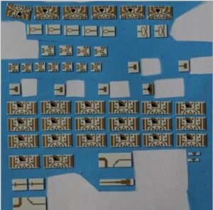
Coraynic Technology Limited supplies BeO ceramics and metallized BeO ceramic components for demanding electronic and industrial applications.
Our capabilities include:
- 99% and 99.5% BeO ceramic
- Customized ceramic geometries
- Mo-Mn and application-specific metallization
- Metallized surfaces and patterns
- Nickel and other specified plating options
- Precision machining
- Ceramic-to-metal brazing
- Hermetic assembly support
- Dimensional and material inspection
- Prototype and production quantities
Metallized BeO components can be developed according to customer drawings, samples, technical specifications, and application requirements.
The final material and process selection should be based on the required thermal performance, electrical characteristics, joining method, operating environment, geometry, and production requirements.
Request a Custom Metallized BeO Ceramic Component
If you are developing a BeO substrate, RF package, feedthrough, hermetic component, or other customized ceramic-metal assembly, Coraynic can evaluate the requirements and recommend a suitable material and metallization approach.
For an RFQ, please provide as much of the following information as available:
- Ceramic material or required BeO grade
- Drawing or CAD file
- Dimensions and tolerances
- Metallization area or pattern
- Plating requirement
- Metal material
- Brazing or soldering method
- Electrical requirements
- Thermal requirements
- Operating environment
- Prototype or annual quantity
Request a Custom Quote for Metallized BeO Ceramic Components
Frequently Asked Questions
What is metallized BeO ceramic?
Metallized BeO ceramic is beryllium oxide ceramic with an engineered metallic layer applied to selected surfaces. The metallized surface can support electrical connection, brazing, soldering, or ceramic-to-metal assembly.
Can BeO ceramic be metallized with Mo-Mn?
Yes. Mo-Mn-based metallization can be used for selected BeO applications where a brazable ceramic-metal interface is required. The exact process should be developed according to the BeO material, geometry, metallization system, plating, and brazing requirements.
What is metallized BeO ceramic used for?
Applications include RF and microwave packages, high-power electronic packaging, vacuum electronic devices, hermetic assemblies, feedthroughs, and other applications requiring thermal management together with electrical insulation and metal integration.
Can metallized BeO ceramic be brazed to metal?
Yes. Properly designed metallization can provide a suitable surface for brazing BeO ceramic to compatible metal components. Joint design, metallization, plating, brazing alloy, thermal expansion, and surface condition must be considered together.
What information is needed for a custom metallized BeO component?
A drawing or CAD file, BeO grade, dimensions, tolerances, metallization pattern, plating requirement, joining method, operating conditions, and expected quantity are useful starting information.
Is BeO safe to machine?
Beryllium-containing dust generated during machining can present serious occupational health hazards. BeO components should therefore be manufactured and machined using appropriate industrial engineering controls and occupational safety procedures. Finished ceramic components and uncontrolled airborne dust should not be treated as equivalent exposure conditions.
Conclusion
Metallized BeO ceramic combines the thermal and electrical characteristics of beryllium oxide with an engineered surface designed for electrical connection, brazing, soldering, or ceramic-to-metal assembly.
Its performance depends on more than the BeO ceramic itself. Material grade, ceramic geometry, metallization system, plating, joining method, thermal expansion, surface condition, and inspection requirements all contribute to the performance of the finished component.
For RF, microwave, high-power electronics, vacuum electronics, and specialized hermetic assemblies, metallized BeO can provide a practical route to integrating high-thermal-conductivity ceramic with metallic structures.
For application-specific requirements, the most reliable approach is to evaluate the ceramic, metallization, joining process, and final operating environment as one engineered system.
Need a custom metallized BeO ceramic component? Contact Coraynic with your drawing, specifications, or application requirements for technical evaluation and quotation.