
Beryllia (BeO) Substrates for High-Power Semiconductor Packaging, IGBT Modules, Microwave Circuits, and LED Heat Sinks
99.5% high-purity beryllium oxide ceramic substrates for RF, microwave, power electronics, semiconductor packaging, and high-power electronic applications.
Coraynic Technology Limited supplies 99.5% Beryllium Oxide (BeO) Ceramic Substrates for electronic applications requiring a combination of high thermal conductivity, electrical insulation, low dielectric loss, and reliable thermal performance.
BeO ceramic is well suited to electronic designs where heat must be efficiently dissipated while maintaining electrical isolation. Its combination of thermal and dielectric properties makes BeO substrates suitable for high-power semiconductor packaging, RF and microwave circuits, power electronic modules, LED thermal management, and other demanding electronic applications.
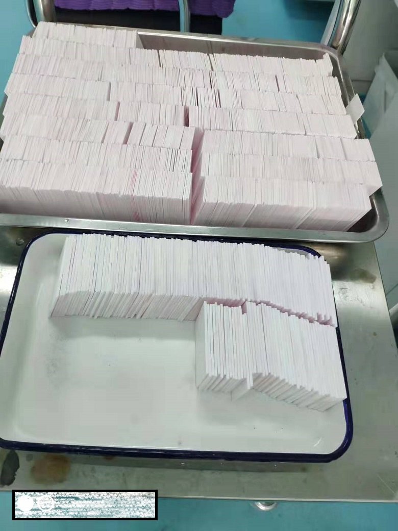
Our BeO ceramic substrates are manufactured from high-purity BeO ceramic material using controlled forming and sintering processes. Precision surface finishing and customized dimensions are available according to customer drawings and application requirements.
Standard substrate sizes can be supplied for selected applications, while custom thicknesses, dimensions, shapes, surface finishes, and metallization configurations can be evaluated for OEM projects.
BeO ceramic provides high thermal conductivity while maintaining electrical insulation. The supplied 99.5% BeO substrate grade can provide thermal conductivity of approximately 285 W/(m·K) at 25°C, depending on material and processing requirements.
With a dielectric constant of approximately 6.6 ± 0.2 at 1 MHz and low dissipation factor, BeO substrates are suitable for high-frequency electronic applications where dielectric performance is important.
BeO provides high volume resistivity and dielectric strength, allowing the substrate to combine thermal management with electrical isolation.
The standard material grade is 99.5% BeO, suitable for demanding electronic and thermal management applications.
Substrates can be manufactured according to customer requirements for thickness, length, width, diameter, surface finish, tolerances, and other dimensional specifications.
BeO substrates can be supplied for further metallization or integrated with metallization processes such as MoMn, thin film, thick film, and other application-specific configurations.
The following values are representative specifications for the 99.5% BeO ceramic substrate grade. Actual values may vary according to material formulation, processing conditions, dimensions, and customer requirements.
| Property | Unit | Value |
|---|---|---|
| Purity | % | 99.5 |
| Density | g/cm³ | ≥2.88 |
| Color | – | White |
| Thermal Conductivity at 25°C | W/(m·K) | 285 |
| Thermal Conductivity at 100°C | W/(m·K) | 220 |
| Dielectric Constant at 1 MHz | – | 6.6 ± 0.2 |
| Dielectric Constant at 10 GHz | – | 6.8 ± 0.2 |
| Dissipation Factor | – | ≤4 × 10⁻⁴ |
| CTE, 25–500°C | ×10⁻⁶/°C | 7.0–8.0 |
| Dielectric Strength | kV/mm | ≥40 |
| Flexural Strength | MPa | ≥200 |
| Compressive Strength | MPa | >350 |
| Young’s Modulus | GPa | 345 |
| Surface Roughness, Ra | μm | 0.05–0.8 |
Specifications should be confirmed according to the selected material grade, substrate geometry, surface finish, and application requirements.
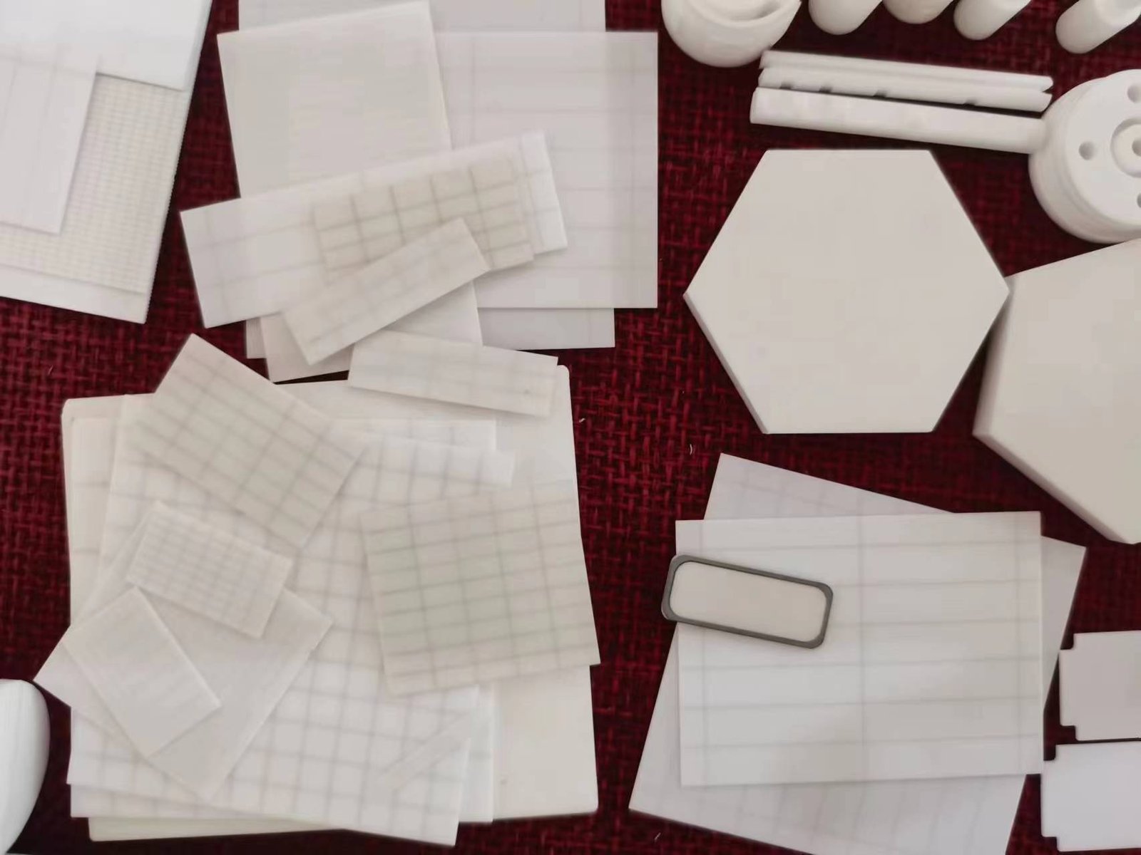
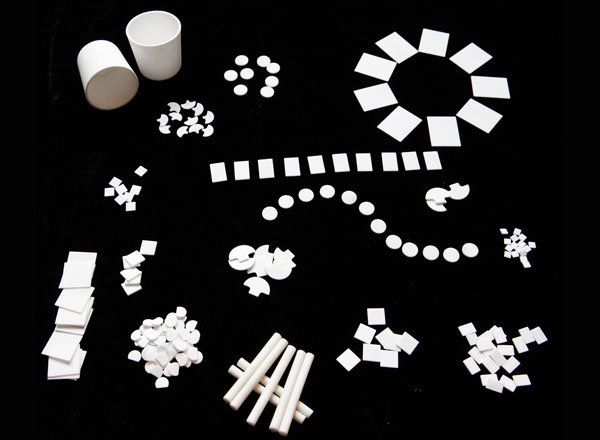
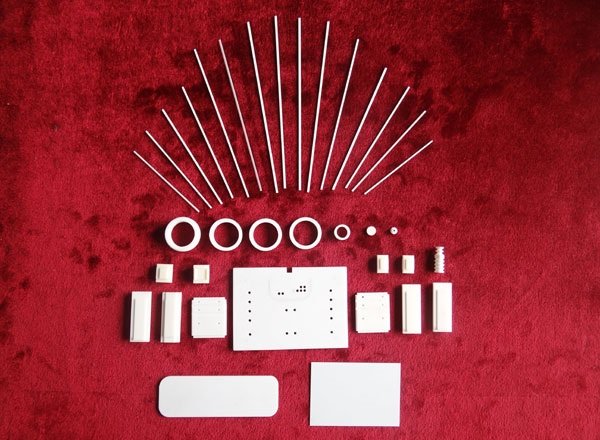
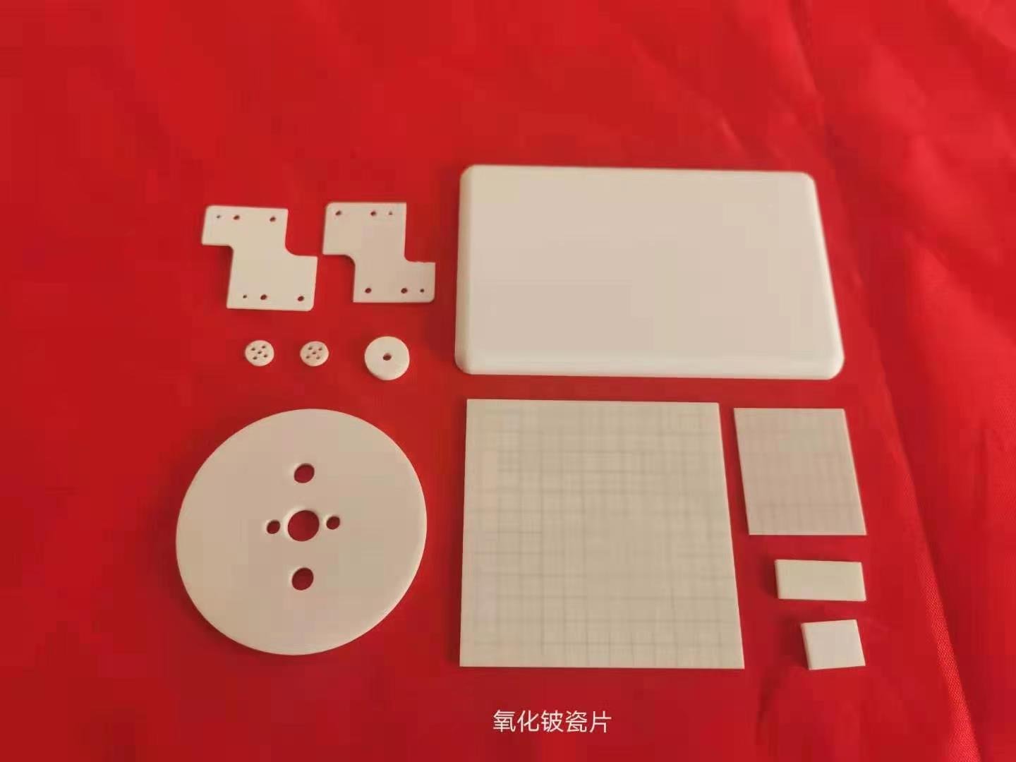
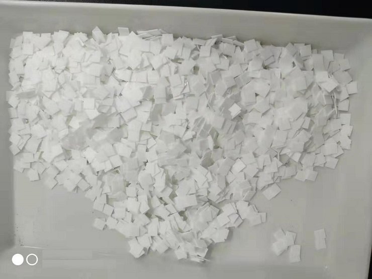
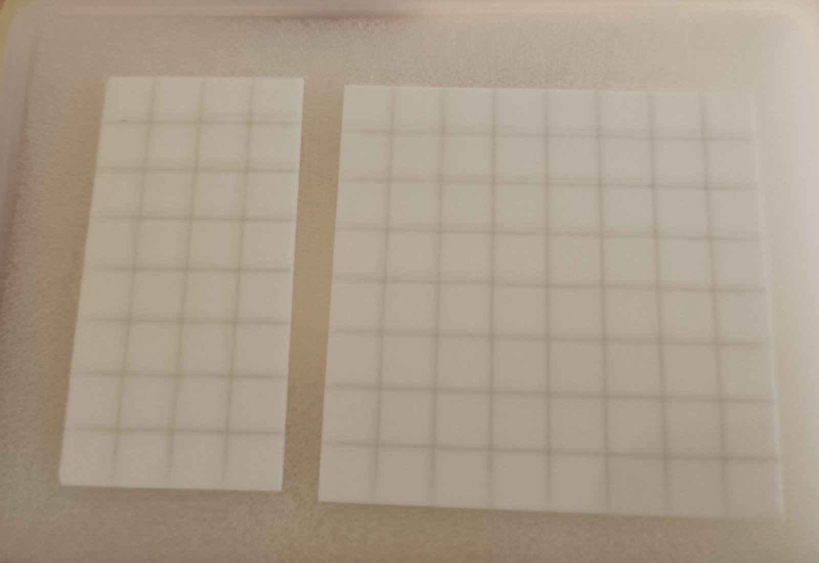
We offer standard square and rectangular BeO ceramic substrates for electronic applications, together with custom manufacturing for non-standard requirements.
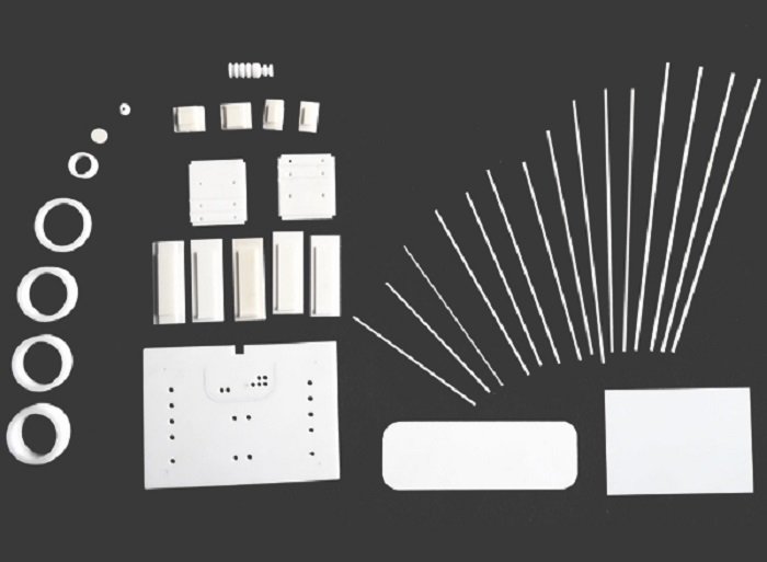
For special applications, additional geometries can be evaluated, including rings, windows, rods, and other application-specific configurations.
Many electronic applications require substrates that cannot be accommodated by standard ceramic dimensions. Coraynic can manufacture BeO substrates according to engineering drawings, CAD files, samples, or technical specifications.
Custom options may include:
Examples of customized dimensions include:
Special dimensions can be reviewed according to the component design, manufacturing process, and production requirements.
BeO ceramic substrates can be supplied with different surface conditions depending on the intended application and metallization requirements.
Available options may include:
Surface roughness requirements can be specified according to the customer’s application, metallization process, bonding method, or assembly requirements.
For electronic packaging and interconnection applications, BeO ceramic substrates can be supplied with optional metallization.
Available metallization technologies may include:
Metallization can be applied to selected areas or designed according to the required electrical and assembly configuration.
For detailed information about metallization processes and customized metallized components, see our Metallized BeO Ceramic page.
BeO ceramic substrates are used where high thermal conductivity and electrical insulation are required in the same component.
BeO substrates are suitable for:
Typical applications include:
BeO substrates can be used in high-power semiconductor packaging where efficient heat dissipation and electrical isolation are required.
Applications may include:
BeO substrates may be used in demanding electronic systems where thermal management, electrical insulation, and dimensional stability are important design considerations.
As electronic devices become smaller and power density increases, thermal management becomes increasingly important.
BeO ceramic substrates provide a combination of:
High Thermal Conductivity + Electrical Insulation + Low Dielectric Loss
This makes them suitable for applications where conventional electrically insulating ceramic substrates may not provide sufficient thermal performance.
For high-power electronic designs, substrate selection can be evaluated according to:
Coraynic can review these parameters when selecting a suitable BeO substrate configuration.
Our BeO substrate manufacturing process can include:
BeO Powder → Forming → Sintering → Grinding / Lapping → Precision Finishing → Inspection
Depending on the product design, additional precision processing can be considered for:
For OEM projects, manufacturing requirements can be developed from customer drawings and technical specifications.
Quality inspection can be performed according to product specifications and customer requirements.
Typical inspection items may include:
Inspection reports and material documentation can be provided according to project requirements.
Coraynic supports custom BeO ceramic substrate projects from prototype quantities to production orders.
Customers can provide:
Our engineering team can review the design and recommend an appropriate BeO material grade, substrate configuration, surface finish, and manufacturing process.
For applications beyond standard BeO ceramic substrates, Coraynic also supplies related BeO ceramic solutions:
BeO Ceramic
General BeO material grades, precision ceramic components, rods, tubes, discs, rings, and custom geometries.
Metallized BeO Ceramic
MoMn, thin-film, thick-film, plating, and customized metallization for electrical connection, brazing, soldering, and electronic packaging.
BeO Ceramic-to-Metal Seal
BeO ceramic integrated with Kovar, oxygen-free copper, MoCu, titanium alloys, and other compatible metals for hermetic and high-reliability assemblies.
Looking for a BeO ceramic substrate for RF, microwave, power electronics, semiconductor packaging, or thermal management?
Send us your drawing, substrate dimensions, thickness, material purity, quantity, surface finish, and metallization requirements.
Coraynic can evaluate your requirements and provide a customized quotation, technical proposal, and production lead time.
Request a BeO Ceramic Substrate Quote →