Ceramic substrates have revolutionized the electronics industry by providing the ideal foundation for high-power, high-frequency, and high-reliability applications. From the indicator lights on your home appliances to the radar systems in fighter jets, ceramic substrates enable the thermal management, electrical insulation, and mechanical support that modern semiconductor devices demand.
But not all ceramic substrates are created equal. The choice between Alumina (Al₂O₃), Aluminum Nitride (AlN), Silicon Carbide (SiC), Beryllium Oxide (BeO), and Low-Temperature Co-Fired Ceramics (LTCC) can fundamentally impact your device’s performance, reliability, and cost.
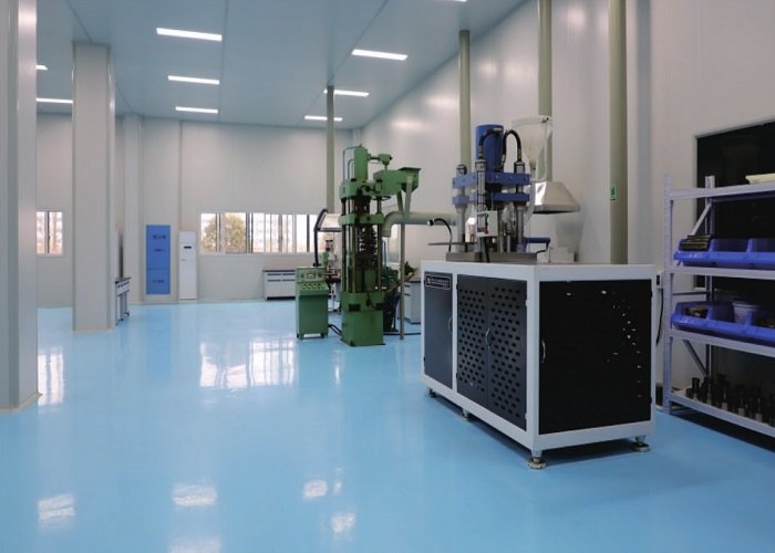
At Coraynic, we specialize in advanced ceramic solutions. This comprehensive guide will help you understand the properties, manufacturing methods, and applications of each major ceramic substrate type, empowering you to make the right choice for your specific design requirements.
1. What is a Ceramic Substrate?
A ceramic substrate iis a flat, rigid sheet material made from electronic-grade ceramics that serves as both a mechanical support and electrical insulator for electronic components. It provides the foundation upon which circuit patterns, semiconductor dies, and passive components are mounted and interconnected.
Why Ceramics?
| Requirement | Why Ceramics Excel |
|---|---|
| Thermal Management | High thermal conductivity efficiently conducts heat away from active devices |
| Electrical Insulation | High dielectric strength and insulation resistance prevent electrical breakdown |
| Thermal Expansion Matching | CTE closely matches silicon and other semiconductor materials |
| Mechanical Strength | High flexural strength supports components and withstands assembly stresses |
| Chemical Stability | Resistant to moisture, chemicals, and oxidation |
| Process Compatibility | Can be metallized, patterned, and multilayered using established processes |
2. Key Properties of Ceramic Substrates
Before diving into specific materials, let us understand the key performance parameters that matter to design engineers:
| Property | What It Means | Why It Matters |
|---|---|---|
| Thermal Conductivity (W/m·K) | Material’s ability to conduct heat | Higher values mean better heat dissipation; critical for high-power devices |
| Dielectric Constant (εr) | Measure of charge storage capability | Lower values reduce signal propagation delay and parasitic capacitance |
| Dielectric Loss (tanδ) | Measure of energy absorbed by the material | Lower values mean less signal attenuation, especially at high frequencies |
| Coefficient of Thermal Expansion (CTE, ppm/°C) | Rate of dimensional change with temperature | Must match attached materials (Si, GaN) to prevent stress fractures |
| Flexural Strength (MPa) | Resistance to bending/breaking | Higher values ensure mechanical durability during assembly and operation |
| Maximum Operating Temperature (°C) | Highest temperature at which material maintains performance | Defines the thermal envelope for high-temperature applications |
3. Manufacturing Methods for Ceramic Substrates
The properties of a ceramic substrate depend not only on its composition but also on how it is manufactured. The four primary forming methods are:
| Method | Process Description | Advantages | Applications |
|---|---|---|---|
| Dry Pressing | Powder is pressed in a die under high pressure | Simple, cost-effective, high production rates | Simple shapes, small substrates |
| Isostatic Pressing | Powder is pressed uniformly using fluid pressure | Uniform density, no orientation effects | High-reliability components |
| Extrusion | Material is forced through a die to create shapes | Continuous production, uniform cross-section | Rods, tubes, complex profiles |
| Tape Casting | Slurry is spread into thin sheets, dried, and cut | Most versatile—enables multilayer structures, high dimensional accuracy | LSI packages, hybrid ICs, multilayered substrates |
Tape casting is particularly important because it enables the creation of multilayer substrates—stacked ceramic layers with internal circuitry, vias, and embedded components. This is the foundation of modern high-density packaging.
4. Types of Ceramic Substrates: A Detailed Comparison
Now, let us examine each major ceramic substrate type in detail.
4.1 Alumina (Al₂O₃) Substrates
The Industry Workhorse
| Parameter | Typical Value (96-99.6%) |
|---|---|
| Thermal Conductivity | 24–30 W/m·K |
| Dielectric Constant | 9.0–10.0 |
| Dielectric Loss | ~0.0004 |
| CTE | ~7.2 ppm/°C |
| Flexural Strength | 300–400 MPa |
| Max Operating Temp | ~1500°C |
Manufacturing:
Raw material (bauxite/aluminite) processed via the Bayer method.
Formed primarily via tape casting with PVB binder.
Fired at 1550–1600°C with sintering aids.
Metallized via thick-film printing or co-firing with refractory metals (W, Mo).
Advantages:
✓ Lowest cost among all ceramic substrates
✓ Mature, well-established manufacturing and metallization technologies
✓ High mechanical strength
✓ Excellent chemical stability
✓ Abundant raw materials
Disadvantages:
✗ Lowest thermal conductivity—limiting for high-power applications
✗ Higher dielectric constant (slower signal propagation)
✗ CTE mismatch with some advanced semiconductors
Applications:
Hybrid integrated circuit substrates
LSI package substrates
Multilayer circuit substrates
General-purpose consumer electronics
4.2 Aluminum Nitride (AlN) Substrates
The High-Performance Thermal Manager
| Parameter | Typical Value |
|---|---|
| Thermal Conductivity | 170–200 W/m·K |
| Dielectric Constant | 8.5–9.0 |
| Dielectric Loss | ~0.0002–0.0005 |
| CTE | ~4.5 ppm/°C |
| Flexural Strength | 300–350 MPa |
| Max Operating Temp | ~1800°C |
Manufacturing:
AlN is an artificial mineral (first synthesized in 1862).
Powder prepared via reduction nitridation (Al₂O₃ + carbon + N₂) or direct nitridation (Al + N₂).
Formed via tape casting with organic binders, then laminated, hot-pressed, degreased, and fired.
Advantages:
✓ Thermal conductivity >10× that of Al₂O₃
✓ CTE closely matches silicon (~4.5 vs. ~3–4 ppm/°C for Si)
✓ Higher insulation resistance and dielectric withstand voltage
✓ Lower dielectric constant than Al₂O₃
Disadvantages:
✗ More expensive than Al₂O₃
✗ Hygroscopic—absorbs moisture, which can degrade performance (especially in humid environments)
✗ Requires specialized processing to achieve high thermal conductivity
Applications:
VHF/UHF power amplifier modules
High-power devices and laser diode substrates
High-power LEDs
IGBT power modules
4.3 Silicon Carbide (SiC) Substrates
The Extreme-Temperature Specialist
| Parameter | Typical Value |
|---|---|
| Thermal Conductivity | 120–270 W/m·K |
| Dielectric Constant | 9.5–10.0 (high) |
| CTE | ~3.7–4.0 ppm/°C |
| Flexural Strength | 400–500 MPa |
| Max Operating Temp | ~2000°C |
Manufacturing:
SiC is an artificial mineral produced by heating silica, coke, and salt to >2000°C.
Difficult to densify—requires sintering aids and specialized methods like vacuum hot pressing.
Advantages:
✓ Highest thermal diffusivity—even higher than copper
✓ CTE very close to silicon
✓ Excellent thermal shock resistance
✓ Exceptional high-temperature stability
✓ Highest mechanical strength
Disadvantages:
✗ High dielectric constant—limits high-frequency applications
✗ Lower dielectric withstand voltage than Al₂O₃/AlN
✗ Difficult and expensive to manufacture (hot pressing required)
✗ Limited metallization options
Applications:
Low-voltage circuits and VLSI high-heat-dissipation substrates
High-speed, high-integration logic LSI with heat dissipation packages
Ultra-large computers
Laser diode substrates for optical communication
High-temperature sensors and MEMS
4.4 Beryllium Oxide (BeO) Substrates
The Thermal-Electrical Champion
| Parameter | Typical Value |
|---|---|
| Thermal Conductivity | 200–325 W/m·K |
| Dielectric Constant | 6.7–7.0 (lowest among high-performance ceramics) |
| Dielectric Loss | <0.0004 |
| CTE | ~7.4 ppm/°C |
| Flexural Strength | 200–220 MPa |
| Max Operating Temp | ~2000°C |
Manufacturing:
BeO is produced via beryllium sulfate crystallization, alkaline beryllium acetate decomposition, or hydrolytic complexation methods.
Primarily formed via dry pressing, though tape casting is possible with additives (MgO or Al₂O₃).
Advantages:
✓ Best combination of high thermal conductivity AND low dielectric constant
✓ Thermal conductivity >10× that of Al₂O₃
✓ Excellent high-temperature stability (2000°C)
✓ CTE well-matched to Si and GaN
✓ Low dielectric loss—ideal for high-frequency applications
✓ Not hygroscopic—unlike AlN, BeO remains stable in humid environments
Disadvantages:
✗ Higher cost than Al₂O₃
✗ Health concerns during powder handling (but sintered product is inert and safe)
✗ Fewer manufacturers than Al₂O₃
Applications:
High-power RF amplifiers and radar systems
Microwave and millimeter-wave communication equipment
Satellite communication systems
High-power semiconductor modules
Traveling wave tubes and vacuum electronics
High-power LED and laser diode packages
Nuclear reactor components (reflectors, moderators)
4.5 Low-Temperature Co-Fired Ceramic (LTCC) Substrates
The Multilayer Integration Solution
| Parameter | Typical Value |
|---|---|
| Thermal Conductivity | 2–4 W/m·K (glass-ceramic composites) |
| Dielectric Constant | 5.0–8.0 (tunable) |
| Dielectric Loss | 0.001–0.005 |
| CTE | 5.0–8.0 ppm/°C (tunable) |
| Firing Temperature | 850–900°C |
| Conductor Metals | Ag, Cu, Au, Ag/Pd |
Manufacturing:
Alumina powder is mixed with 30–50% glass material and organic binders to form a slurry.
Tape casting produces green sheets.
Vias are laser-drilled and filled with metal paste.
Screen printing patterns circuit layers.
Sheets are laminated and co-fired at 850–900°C.
Advantages:
✓ Low firing temperature enables use of low-resistivity metals (Ag, Cu, Au)
✓ Multilayer capability—up to 50+ layers with embedded passive components
✓ Tunable properties—dielectric constant and CTE can be tailored
✓ Excellent high-frequency performance (RF, microwave, millimeter-wave)
✓ Fine-pitch wiring capability
Disadvantages:
✗ Lower thermal conductivity than BeO, AlN, or SiC
✗ More complex and expensive manufacturing process
✗ Shrinkage during firing must be carefully controlled
✗ Glass phase can limit long-term stability at very high temperatures
Applications:
Multilayer substrates for supercomputers
Automotive ECU modules (engine control units)
RF and microwave modules—VCO, TCXO, filters, duplexers
Optical communication interface modules
HEMT modules
5G/mmWave front-end modules
Medical implantable devices
5. Comparison Summary: Choosing the Right Substrate
| Substrate | Thermal Conductivity | Dielectric Constant | CTE (ppm/°C) | Cost | Best For |
|---|---|---|---|---|---|
| Al₂O₃ | Low (24–30) | High (9–10) | ~7.2 | $ | General-purpose, cost-sensitive applications |
| AlN | High (170–200) | Medium (8.5–9) | ~4.5 | $$$ | High-power, CTE-matched to Si |
| SiC | High–Very High (120–270) | High (9.5–10) | ~3.7–4.0 | $$$$ | Extreme temperatures, high mechanical stress |
| BeO | Very High (200–325) | Low (6.7–7.0) | ~7.4 | $$$ | High-power AND high-frequency combined |
| LTCC | Low–Medium (2–4) | Tunable (5–8) | Tunable | $$$ | Multilayer integration, RF/microwave modules |
6. The Future of Ceramic Substrates
As GaN, SiC, and next-generation semiconductors push power densities ever higher, the demand for advanced ceramic substrates continues to grow. Key trends include:
Higher Thermal Conductivity: Development of new compositions and processing methods to push BeO and AlN performance further.
Integration: LTCC and multilayer technologies enabling system-in-package (SiP) solutions.
Miniaturization: Finer vias, narrower lines, and higher layer counts.
Cost Reduction: Advances in manufacturing making BeO and AlN more accessible.
Sustainability: Development of recycling and waste-reduction processes for ceramic manufacturing.
7. Why Coraynic?
At Coraynic, we bring deep expertise across the full spectrum of ceramic substrate technologies:
Specialization: We focus on high-performance materials—particularly BeO and advanced alumina ceramics.
Quality: Rigorous process control and inspection (including X-ray NDT) ensure reliability.
Customization: We deliver substrates tailored to your exact specifications—dimensions, metallization, and tolerances.
Technical Support: Our team assists with material selection, design optimization, and process integration.
Global Reach: Flexible supply serving customers worldwide, from prototyping to volume production.
8. Conclusion: Make the Right Choice with Coraynic
Selecting the right ceramic substrate is one of the most consequential decisions you will make in designing a high-performance electronic system. The choice affects thermal management, signal integrity, mechanical reliability, and ultimately, the success of your product in the field.
Whether your application demands the thermal-electrical excellence of BeO, the cost-effectiveness of Alumina, the CTE match of AlN, the extreme durability of SiC, or the integration capability of LTCC, Coraynic has the expertise to guide you.
Ready to Choose Your Ceramic Substrate?
📧 Contact us today for technical consultation, samples, or custom quotations.
🌐 Visit us at: www.coraynic.com