Precision Metallized Beryllia Ceramics for High-Power RF, Microwave Vacuum Devices, Hermetic Packaging, and Thin-Film Circuits
Beryllium Oxide (BeO) ceramic is the material of choice when extreme thermal management and electrical insulation are required. With thermal conductivity up to 310 W/m·K (second only to diamond) and a low dielectric constant of 6.6–6.9, BeO is indispensable in high-power, high-frequency applications.
Coraynic Technology offers 99.5% highpurity BeO ceramics with two advanced metallization options:
- MoMn + Nickel Plating – Thickfilm metallization for hermetic sealing, brazing, and high-reliability packaging (military/aerospace, power electronics).
- ThinFilm Metallization via Vacuum Magnetron Sputtering – Precision patterned metal layers (Ti/Pt/Au, NiCr, etc.) for high-density circuits, wire bonding, and RF/microwave components.
Both processes preserve the intrinsic properties of the BeO substrate while providing excellent adhesion, solderability, wire bondability, and hermeticity.
Key Features & Benefits
UltraHigh Thermal Conductivity 285–310 W/m·K – 12× Al₂O₃, 1.7× AlN
Low Dielectric Loss 6.6–6.9 @1MHz, tan δ ≤4×10⁻⁴ – ideal for RF/microwave
CTE Matched to Semiconductors 7.0–9.2 ×10⁻⁶/°C – compatible with Si, GaAs, GaN, kovar
MoMn + Ni Plating 15–38 µm MoMn + 2–10 µm Ni – high bond strength, hermetic, solderable
ThinFilm Sputtering 0.1–5 µm precision layers – Ti/Pt/Au, NiCr, TiW/Au, etc.
Vacuum Magnetron Sputtering Uniform, dense, pin-hole-free films – excellent adhesion
Pattern Customization Full-surface, selective area, edge wraps, via holes, laser scribing
Hermetic Sealing Capable <5×10⁻¹² Pa·m³/s – vacuumtight, suitable for brazing/welding
Wire Bond Ready Gold flash surface – 25 µm Al wire, 50 µm Au wire compatible
High Reliability Passes 1000+ thermal cycles (55°C to +150°C)
Technical Specifications (99.5% BeO Base Material)
Property Unit Value
Purity:99.5 %
Density g/cm³ 2.88–3.05
Color – White
Thermal Conductivity (25°C) W/m·K 285–310
Thermal Conductivity (100°C) W/m·K 220
Dielectric Constant (1MHz) – 6.6 ±0.2
Dielectric Constant (10GHz) – 6.8 ±0.2
Dissipation Factor (1MHz) – ≤4×10⁻⁴
CTE (25–500°C) ×10⁻⁶/°C 7.0–9.2
Volume Resistivity (25°C) Ω·cm >10¹⁴
Dielectric Strength (DC) kV/mm ≥25–40
Flexural Strength MPa ≥200
Compressive Strength MPa >350
Surface Roughness (Ra) – as fired μm 0.2–0.8
Surface Roughness (Ra) – polished μm <0.1
Camber ‰ ≤2
Air Tightness Pa·m³/s ≤5×10⁻¹²
Grain Size μm 10–20
Metallization Option 1: MoMn + Nickel Plating Process Description
The MoMn (Molybdenum Manganese) process is a thick-film metallization method widely used for high-reliability ceramic-to-metal sealing. A MoMn paste is screenprinted or coated onto the BeO surface and sintered at ≤1550°C in a controlled atmosphere, forming a strong chemical bond with the ceramic.
A nickel plating layer (2–10 µm) is then applied to protect the MoMn and provide a solderable, brazable surface. Optional gold flash (0.05–0.3 µm) can be added for oxidation resistance and wire bonding.
Specifications – MoMn + Ni Plating
Parameter Value
Metallization Material MoMn (MolybdenumManganese)
MoMn Thickness 15–38 µm
Nickel Plating Thickness 2–10 µm
Gold Flash (optional) 0.05–0.3 µm
Sintering Temperature ≤1550°C (optimized for BeO preservation)
Peel Strength (90° peel, 50 mm/min) >15 N/mm (on Al₂O₃); >12 N/mm on BeO
Sealing Strength (brazed joint) ≥30 MPa
Solderability >95% wetting rate (Au/Sn, Ag/Cu)
Hermeticity <5×10⁻¹² Pa·m³/s
Thermal Cycling >1000 cycles (55°C to +150°C)
Applications – MoMn + Ni Plating
Defense & Aerospace Radar T/R modules, traveling wave tube (TWT) components, missile guidance
Telecommunications Highpower RF transistor packages (GaN, GaAs), base station amplifiers
Power Electronics IGBT modules, high-current feedthroughs, power hybrid circuits
Medical X-ray tube insulators, gas laser cavities
Nuclear Hermetic feedthroughs for instrumentation
Metallization Option 2: ThinFilm via Vacuum Magnetron Sputtering
Process Description
Vacuum Magnetron Sputtering is a physical vapor deposition (PVD) technique used to deposit ultrathin, highly uniform metal films onto BeO ceramic substrates. The process takes place in a high vacuum chamber where a plasma is generated to eject atoms from a target material, which then condense onto the substrate.
This method enables:
Precision thickness control (angstrom to micron level)
Excellent adhesion without high-temperature sintering
Fineline patterning (down to 10–20 µm line/space)
Multilayer stacks (e.g., Ti/Pt/Au, NiCr/Au, TiW/Au)
Low thermal budget – no damage to BeO properties
Typical ThinFilm Layer Stacks
Stack Layer 1 Layer 2 Layer 3 Application
Ti/Pt/Au Ti: 50–100 nm Pt: 100–200 nm Au: 200–1000 nm Wire bonding, eutectic die attach
NiCr/Au NiCr: 100–300 nm Au: 300–1000 nm – Resistors, bond pads
TiW/Au TiW: 100–300 nm Au: 300–2000 nm – Diffusion barrier, high-temperature
Cr/Au Cr: 50–100 nm Au: 200–1000 nm – General purpose metallization
TaN/TiW/Au TaN: 50–100 nm TiW: 100–300 nm Au: 300–2000 nm Precision resistors, stable contacts
Specifications – ThinFilm Sputtering
Parameter Value
Film Thickness Range 0.01–5 µm (10 nm – 5 µm)
Thickness Tolerance ±5% (for <1 µm), ±10% (for >1 µm)
Minimum Line Width 10–20 µm (depending on photolithography)
Minimum Line Spacing 10–20 µm
Adhesion (tape test) 5/5 (no peeling)
Wire Bond Strength >10 gf (25 µm Al wire), >50 gf (50 µm Au wire)
Resistivity (Au) 2.2–3.0 µΩ·cm
Surface Roughness (Ra) <0.05 µm (on polished BeO)
Patterning Method Photolithography + liftoff or etching
Applications – ThinFilm Sputtering
Industry Application
RF & Microwave Highfrequency substrates, microstrip circuits, filters, couplers
Optoelectronics Laser diode submounts, photodiode packages, VCSEL arrays
Semiconductor Wafer probing cards, MEMS packaging, sensor interfaces
Medical Implantable device feedthroughs, microelectrode arrays
Quantum Computing Cryogenic microwave resonators, qubit control lines
Research & Development Custom test structures, prototype circuits
Comparison: MoMn + Ni Plating vs. ThinFilm Sputtering
Feature MoMn + Ni Plating ThinFilm Sputtering
Layer Thickness 15–50 µm (thick film) 0.01–5 µm (thin film)
Minimum Feature Size 100–300 µm 10–20 µm
Adhesion Mechanism chemical bond via sintering Physical bond via sputtering
Process Temperature 1300–1550°C <200°C
Surface Roughness Follows substrate roughness Can planarize, very smooth
Solderability Excellent (thick Ni/Au) Good (requires thicker Au for soldering)
Wire Bonding Good (Au flash) Excellent (smooth, pure Au)
Hermetic Sealing Excellent (brazing) Limited to thin-film sealing layers
Best For Power packages, hermetic feedthroughs, high current High frequency circuits, fineline patterns, sensors
Standard & Custom Sizes
Substrates (Rectangular / Square)
Thickness (mm) Length × Width (mm)
0.254 (0.010″) 25.4 × 25.4 (1″×1″)
0.385 50.8 × 50.8 (2″×2″)
0.5 76.2 × 76.2 (3″×3″)
0.635 101.6 × 101.6 (4″×4″)
1.0 114.3 × 114.3 (4.5″×4.5″)
1.5 Custom dimensions
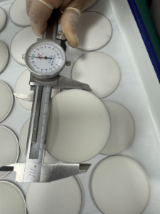
Disc / Round Substrates
Diameter (mm) : 20, 26, 30, 35, 50, 52, 60, 75, 100, 110
Thickness Range (mm): 0.25 – 2.0
Custom Shapes & Features
Component Type Options
Rods Traveling wave tube supports, clamping bars
Cylinders / Tubes Feedthrough insulators, vacuum envelopes
Windows Microwave transmission windows (Cband, Xband)
Rings Hermetic sealing spacers, ball rings
Custom Profiles Stepped, tapered, flanged, threaded, notched
Metallization Patterns Full surface, selective areas, edge wraps, via holes, laser scribing
Successful Project Examples
✅ Project 1: Metallized BeO Disc / Ball / Ring for CBand Window
Components: DiscBallRing (Ø66*/3.2 mm)
Metallization: MoMn + Ni
Application: Highpower microwave window in Cband window
Outcome: Hermeticity <5×10⁻¹² Pa·m³/s, passed 1000 thermal cycles
✅ Project 2: BeO Substrate with MoMn + Flash Gold for laser Package
Substrate: 22 × 12 × 2 mm
Metallization: MoMn (7.6217.78 µm) + Ni (2.543.81µm) + Au flash (0.8~1.3 µm)
Application: laser electronics
Outcome: 98% yield, 22°C lower junction temperature vs. AlN
✅ Project 3: Thin-Film Sputtered BeO for Microwave Integrated Circuit
Substrate:11*11*1.10mm. MoMn1015um, Nikel:1.3~2.0um
Application: Xband microstrip filter
Outcome: Line width 20 µm, insertion loss <0.5 dB at 10 GHz
Engineering Capability
✅ Manufacturing Equipment
Equipment Function
Vacuum Magnetron Sputtering System Multitarget, DC/RF, up to 200 mm wafer size
MoMn Screen Printing & Sintering Line 1550°C controlled atmosphere furnaces
Nickel/Gold Plating Line Electrolytic and electroless, thickness control ±1 µm
CNC Precision Grinding Flatness <0.035 mm, camber ≤2‰
Laser Cutting & Drilling Via holes, scribing, contour cutting ±0.01 mm
Photolithography Suite UV exposure, spin coating, developing – 10 µm resolution
Ultrasonic Machining Complex 3D shapes, brittle materials
✅ Metrology & Quality Assurance
Instrument Application
ICP Plasma Spectrometer Purity analysis, trace element detection
Laser Particle Analyzer Powder particle size distribution
Universal Tool Microscope Dimensional inspection, edge quality
Surface Roughness Tester Ra, Rz verification
Helium Leak Detector Air tightness testing (<5×10⁻¹² Pa·m³/s)
Thermal Conductivity Meter Laser flash method (25°C–1000°C)
Dielectric Strength Tester HV breakdown verification
Wire Bond Pull Tester Bond strength validation
CMM (Coordinate Measuring Machine) 3D dimensional tolerance certification
Scanning Electron Microscope (SEM) Film morphology, crosssection analysis
Why Choose Coraynic Technology?
Vertically Integrated: From BeO powder to metallized finished component – all inhouse.
Dual Metallization Expertise: Both thickfilm (MoMn) and thinfilm (sputtering) capabilities.
Defense & Aerospace Qualified: Supplier to stateowned defense enterprises; ITAR compliant.
Custom Engineering: Our team assists with pattern design, film stack selection, and brazing compatibility.
Process Control: 100% QC with advanced analytics – ICP, helium leak detection, SEM.
Global Shipping: UN 1566 6.1/PG 2 certified packaging for BeO products.
Compliance: RoHS, CE, REACH. Full SDS and material traceability provided.
Contact Our Engineering Team
📱 Mobile (WhatsApp / WeChat): +86 187 6195 1906
📧 Email (General Inquiries): `info@coraynic.com`
📧 Email (Sales & Quotations): `sales@coraynic.com`
🌐 Website: `www.coraynic.com`