Subtitle:
Precision Metallized Beryllia Ceramics for High-Power RF, Microwave Vacuum Devices, Hermetic Packaging, and Thin-Film Circuits
Beryllium Oxide (BeO) ceramic is the material of choice when extreme thermal management and electrical insulation are required. With thermal conductivity up to 310 W/m·K (second only to diamond) and a low dielectric constant of 6.6–6.9, BeO is indispensable in high-power, high-frequency applications.
Coraynic Technology offers 99.5% high-purity BeO ceramics with two advanced metallization options:
- MoMn + Nickel Plating – Thick-film metallization for hermetic sealing, brazing, and high-reliability packaging (military/aerospace, power electronics).
- Thin-Film Metallization via Vacuum Magnetron Sputtering – Precision patterned metal layers (Ti/Pt/Au, NiCr, etc.) for high-density circuits, wire bonding, and RF/microwave components.
Both processes preserve the intrinsic properties of the BeO substrate while providing excellent adhesion, solderability, wire bondability, and hermeticity.
—
Key Features & Benefits
| Feature | Benefit |
|———|———|
| Ultra-High Thermal Conductivity | 285–310 W/m·K – 12× Al₂O₃, 1.7× AlN |
| Low Dielectric Loss | 6.6–6.9 @1MHz, tan δ ≤4×10⁻⁴ – ideal for RF/microwave |
| CTE Matched to Semiconductors | 7.0–9.2 ×10⁻⁶/°C – compatible with Si, GaAs, GaN, kovar |
| MoMn + Ni Plating | 15–38 µm MoMn + 2–10 µm Ni – high bond strength, hermetic, solderable |
| Thin-Film Sputtering | 0.1–5 µm precision layers – Ti/Pt/Au, NiCr, TiW/Au, etc. |
| Vacuum Magnetron Sputtering | Uniform, dense, pinhole-free films – excellent adhesion |
| Pattern Customization | Full surface, selective area, edge wraps, via holes, laser scribing |
| Hermetic Sealing Capable | <5×10⁻¹² Pa·m³/s – vacuum-tight, suitable for brazing/welding |
| Wire Bond Ready | Gold flash surface – 25 µm Al wire, 50 µm Au wire compatible |
| High Reliability | Passes 1000+ thermal cycles (-55°C to +150°C) |
—
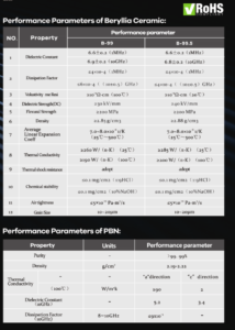
Technical Specifications (99.5% BeO Base Material)
| Property | Unit | Value |
|———-|——|——-|
| Purity | % | 99.5 |
| Density | g/cm³ | 2.88–3.05 |
| Color | – | White |
| Thermal Conductivity (25°C) | W/m·K | 285–310 |
| Thermal Conductivity (100°C) | W/m·K | 220 |
| Dielectric Constant (1MHz) | – | 6.6 ±0.2 |
| Dielectric Constant (10GHz) | – | 6.8 ±0.2 |
| Dissipation Factor (1MHz) | – | ≤4×10⁻⁴ |
| CTE (25–500°C) | ×10⁻⁶/°C | 7.0–9.2 |
| Volume Resistivity (25°C) | Ω·cm | >10¹⁴ |
| Dielectric Strength (DC) | kV/mm | ≥25–40 |
| Flexural Strength | MPa | ≥200 |
| Compressive Strength | MPa | >350 |
| Surface Roughness (Ra) – as fired | μm | 0.2–0.8 |
| Surface Roughness (Ra) – polished | μm | <0.1 |
| Camber | ‰ | ≤2 |
| Air Tightness | Pa·m³/s | ≤5×10⁻¹² |
| Grain Size | μm | 10–20 |
—
Metallization Option 1: MoMn + Nickel Plating
Process Description
The MoMn (Molybdenum-Manganese) process is a thick-film metallization method widely used for high-reliability ceramic-to-metal sealing. A MoMn paste is screen-printed or coated onto the BeO surface and sintered at ≤1550°C in a controlled atmosphere, forming a strong chemical bond with the ceramic.
A nickel plating layer (2–10 µm) is then applied to protect the MoMn and provide a solderable, brazable surface. Optional gold flash (0.05–0.3 µm) can be added for oxidation resistance and wire bonding.
Specifications – MoMn + Ni Plating
| Parameter | Value |
|———-|——-|
| Metallization Material | MoMn (Molybdenum-Manganese) |
| MoMn Thickness | 15–38 µm |
| Nickel Plating Thickness | 2–10 µm |
| Gold Flash (optional) | 0.05–0.3 µm |
| Sintering Temperature | ≤1550°C (optimized for BeO preservation) |
| Peel Strength (90° peel, 50 mm/min) | >15 N/mm (on Al₂O₃); >12 N/mm on BeO |
| Sealing Strength (brazed joint) | ≥30 MPa |
| Solderability | >95% wetting rate (Au/Sn, Ag/Cu) |
| Hermeticity | <5×10⁻¹² Pa·m³/s |
| Thermal Cycling | >1000 cycles (-55°C to +150°C) |
Applications – MoMn + Ni Plating
| Industry | Application |
|———-|————-|
| Defense & Aerospace | Radar T/R modules, traveling wave tube (TWT) components, missile guidance |
| Telecommunications | High-power RF transistor packages (GaN, GaAs), base station amplifiers |
| Power Electronics | IGBT modules, high-current feedthroughs, power hybrid circuits |
| Medical | X-ray tube insulators, gas laser cavities |
| Nuclear | Hermetic feedthroughs for instrumentation |
—
Metallization Option 2: Thin-Film via Vacuum Magnetron Sputtering
Process Description
Vacuum Magnetron Sputtering is a physical vapor deposition (PVD) technique used to deposit ultra-thin, highly uniform metal films onto BeO ceramic substrates. The process takes place in a high-vacuum chamber where a plasma is generated to eject atoms from a target material, which then condense onto the substrate.
This method enables:
– Precision thickness control (angstrom to micron level)
– Excellent adhesion without high-temperature sintering
– Fine-line patterning (down to 10–20 µm line/space)
– Multi-layer stacks (e.g., Ti/Pt/Au, NiCr/Au, TiW/Au)
– Low thermal budget – no damage to BeO properties
Typical Thin-Film Layer Stacks
| Stack | Layer 1 | Layer 2 | Layer 3 | Application |
|——-|———|———|———|————-|
| Ti/Pt/Au | Ti: 50–100 nm | Pt: 100–200 nm | Au: 200–1000 nm | Wire bonding, eutectic die attach |
| NiCr/Au | NiCr: 100–300 nm | Au: 300–1000 nm | – | Resistors, bond pads |
| TiW/Au | TiW: 100–300 nm | Au: 300–2000 nm | – | Diffusion barrier, high-temperature |
| Cr/Au | Cr: 50–100 nm | Au: 200–1000 nm | – | General-purpose metallization |
| TaN/TiW/Au | TaN: 50–100 nm | TiW: 100–300 nm | Au: 300–2000 nm | Precision resistors, stable contacts |
Specifications – Thin-Film Sputtering
| Parameter | Value |
|———-|——-|
| Film Thickness Range | 0.01–5 µm (10 nm – 5 µm) |
| Thickness Tolerance | ±5% (for <1 µm), ±10% (for >1 µm) |
| Minimum Line Width | 10–20 µm (depending on photolithography) |
| Minimum Line Spacing | 10–20 µm |
| Adhesion (tape test) | 5/5 (no peeling) |
| Wire Bond Strength | >10 gf (25 µm Al wire), >50 gf (50 µm Au wire) |
| Resistivity (Au) | 2.2–3.0 µΩ·cm |
| Surface Roughness (Ra) | <0.05 µm (on polished BeO) |
| Patterning Method | Photolithography + lift-off or etching |
Applications – Thin-Film Sputtering
| Industry | Application |
|———-|————-|
| RF & Microwave | High-frequency substrates, microstrip circuits, filters, couplers |
| Optoelectronics | Laser diode submounts, photodiode packages, VCSEL arrays |
| Semiconductor | Wafer probing cards, MEMS packaging, sensor interfaces |
| Medical | Implantable device feedthroughs, microelectrode arrays |
| Quantum Computing | Cryogenic microwave resonators, qubit control lines |
| Research & Development | Custom test structures, prototype circuits |
Comparison: MoMn + Ni Plating vs. Thin-Film Sputtering
| Feature | MoMn + Ni Plating | Thin-Film Sputtering |
|———|——————-|———————-|
| Layer Thickness | 15–50 µm (thick film) | 0.01–5 µm (thin film) |
| Minimum Feature Size | 100–300 µm | 10–20 µm |
| Adhesion Mechanism | Chemical bond via sintering | Physical bond via sputtering |
| Process Temperature | 1300–1550°C | <200°C |
| Surface Roughness | Follows substrate roughness | Can planarize, very smooth |
| Solderability | Excellent (thick Ni/Au) | Good (requires thicker Au for soldering) |
| Wire Bonding | Good (Au flash) | Excellent (smooth, pure Au) |
| Hermetic Sealing | Excellent (brazing) | Limited to thin-film sealing layers |
| Best For | Power packages, hermetic feedthroughs, high-current | High-frequency circuits, fine-line patterns, sensors |
Standard & Custom Sizes
Substrates (Rectangular / Square)
| Thickness (mm) | Length × Width (mm) |
|—————-|———————|
| 0.254 (0.010″) | 25.4 × 25.4 (1″×1″) |
| 0.385 | 50.8 × 50.8 (2″×2″) |
| 0.5 | 76.2 × 76.2 (3″×3″) |
| 0.635 | 101.6 × 101.6 (4″×4″) |
| 1.0 | 114.3 × 114.3 (4.5″×4.5″) |
| 1.5 | Custom dimensions |
Disc / Round Substrates
| Diameter (mm) | Thickness Range (mm) |
|—————|———————-|
| 20, 26, 30, 35, 50, 52, 60, 75, 100, 110 | 0.25 – 2.0 |
Custom Shapes & Features
| Component Type | Options |
|—————-|———|
| Rods | Traveling wave tube supports, clamping bars |
| Cylinders / Tubes | Feedthrough insulators, vacuum envelopes |
| Windows | Microwave transmission windows (C-band, X-band) |
| Rings | Hermetic sealing spacers, ball rings |
| Custom Profiles | Stepped, tapered, flanged, threaded, notched |
| Metallization Patterns | Full surface, selective areas, edge wraps, via holes, laser scribing |
Successful Project Examples
✅ Project 1: Metallized BeO Disc / Ball / Ring for C-Band Window
– Components: Disc-Ball-Ring (Ø66*/3.2 mm)
– Metallization: MoMn + Ni
– Application: High-power microwave window in C-band window
– Outcome: Hermeticity <5×10⁻¹² Pa·m³/s, passed 1000 thermal cycles
✅ Project 2: BeO Substrate with MoMn + Flash Gold for laser Package
– Substrate: 22 × 12 × 2 mm
– Metallization: MoMn (7.62-17.78 µm) + Ni (2.54-3.81µm) + Au flash (0.8~1.3 µm)
– Application: laser electronics
– Outcome: 98% yield, 22°C lower junction temperature vs. AlN
✅ Project 3: Thin-Film Sputtered BeO for Microwave Integrated Circuit
-Substrate:11*11*1.10mm. MoMn10-15um, Nikel:1.3~2.0um
– Application: X-band microstrip filter
– Outcome: Line width 20 µm, insertion loss <0.5 dB at 10 GHz
Engineering Capability
✅ Manufacturing Equipment
| Equipment | Function |
|———-|———-|
| Vacuum Magnetron Sputtering System | Multi-target, DC/RF, up to 200 mm wafer size |
| MoMn Screen Printing & Sintering Line | 1550°C controlled atmosphere furnaces |
| Nickel/Gold Plating Line | Electrolytic and electroless, thickness control ±1 µm |
| CNC Precision Grinding | Flatness <0.035 mm, camber ≤2‰ |
| Laser Cutting & Drilling | Via holes, scribing, contour cutting ±0.01 mm |
| Photolithography Suite | UV exposure, spin coating, developing – 10 µm resolution |
| Ultrasonic Machining | Complex 3D shapes, brittle materials |
✅ Metrology & Quality Assurance
| Instrument | Application |
|———–|————-|
| ICP Plasma Spectrometer | Purity analysis, trace element detection |
| Laser Particle Analyzer | Powder particle size distribution |
| Universal Tool Microscope | Dimensional inspection, edge quality |
| Surface Roughness Tester | Ra, Rz verification |
| Helium Leak Detector | Air tightness testing (<5×10⁻¹² Pa·m³/s) |
| Thermal Conductivity Meter | Laser flash method (25°C–1000°C) |
| Dielectric Strength Tester | HV breakdown verification |
| Wire Bond Pull Tester | Bond strength validation |
| CMM (Coordinate Measuring Machine) | 3D dimensional tolerance certification |
| Scanning Electron Microscope (SEM) | Film morphology, cross-section analysis |
—
Why Choose Coraynic Technology?
– Vertically Integrated: From BeO powder to metallized finished component – all in-house.
– Dual Metallization Expertise: Both thick-film (MoMn) and thin-film (sputtering) capabilities.
– Defense & Aerospace Qualified: Supplier to state-owned defense enterprises; ITAR compliant.
– Custom Engineering: Our team assists with pattern design, film stack selection, and brazing compatibility.
– Process Control: 100% QC with advanced analytics – ICP, helium leak detection, SEM.
– Global Shipping: UN 1566 6.1/PG 2 certified packaging for BeO products.
– Compliance: RoHS, CE, REACH. Full SDS and material traceability provided.