Ceramic substrate material for electronic packaging and its manufacturing
Ceramic substrates due to their good thermal conductivity, heat resistance, insulation, low coefficient of thermal expansion, and continuous decrease in cost, have been used in electronic packaging.
Ceramic substrates mainly include beryllium oxide (BeO), aluminum oxide (Al2O3), aluminum nitride (AlN), and silicon nitride (Si3N4). Compared with other ceramic materials, Si3N4 ceramic substrates have high electrical insulation properties and chemical stability, good thermal stability, and high mechanical strength, and can be used to manufacture highly integrated large-scale circuit boards.
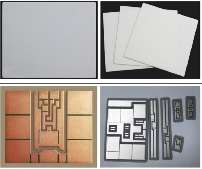
From the perspective of structure and manufacturing process, ceramic substrates can be divided into HTCC, LTCC, TFC, DBC, DPC, and so on.
High-temperature co-fired multilayer ceramic substrate (HTCC)
HTCC, is also known as high-temperature co-fired multilayer ceramic substrate. In the preparation process, ceramic powder (Al2O3 or AlN) is first added to the organic binder, and mixed into a paste slurry, and then the slurry is scraped into flakes by a scraper, and then the flake slurry is formed into a green body by a drying process; Then, through-holes are drilled according to the design of each layer, and the screen printing metal paste is used for wiring and hole filling. Finally, the green layers are stacked and sintered in a high-temperature furnace (1600 ° C).
Due to the high sintering temperature in this preparation process, the choice of metal conductor materials is limited (main metals such as tungsten, molybdenum, and manganese, which have high melting points but poor conductivity), high production costs, and thermal conductivity are generally 20 ~ 200W / (M · ℃).
Low-temperature co-fired ceramic substrate (LTCC)
LTCC, also known as low-temperature co-fired ceramic substrate, has a similar preparation process to HTCC, except that a low melting point glass frit with a mass fraction of 30% to 50% is mixed in Al2O3 powder to reduce the sintering temperature to 850 to 900 ° C, so it can be conductive Good rate of gold and silver as electrode materials and wiring materials.
Because LTCC uses screen-printing technology to make metal circuits, it may cause alignment errors due to the problem of stretching the screen; and there is still a problem of difference in shrinkage ratio when multilayer ceramics are laminated and sintered, which affects the yield. In order to improve the thermal conductivity of LTCC, thermal or conductive holes can be added in the patch area, but the cost increases.
Thick film ceramic substrate (TFC)
Compared to LTCC and HTCC, TFC is a post-fired ceramic substrate. The metal paste is coated on the surface of the ceramic substrate by screen printing technology and is prepared after drying and sintering at high temperatures (700 ~ 800 ° C). The metal paste is generally composed of metal powder, organic resin, and glass. After high-temperature sintering, the resin binder is burned away, and almost all of the remaining is pure metal, which is caused by the glassy adhesion on the surface of the ceramic substrate. The thickness of the sintered metal layer is 10-20 μm, and the minimum line width is 0.3 mm.
As the technology is mature, the process is simple, and the cost is low, TFC has been used in electronic packaging that does not require high graphics accuracy.
Direct Bonded Copper Ceramic Substrate (DBC)
It is formed by the eutectic sintering of a ceramic substrate and copper foil at a high temperature (1065 ° C), and finally, a circuit is formed by etching according to the wiring requirements. The copper foil has good electrical and thermal conductivity, while alumina can effectively control the expansion of the Cu-Al2O3-Cu composite so that the DBC substrate has a thermal expansion coefficient similar to that of alumina.
DBC has the advantages of good thermal conductivity, strong insulation, and high reliability. It has been widely used in IGBT, LD, and CPV packages. The disadvantage of DBC is that it utilizes the eutectic reaction between Cu and Al2O3 at high temperatures, which requires higher equipment and process control and higher substrate cost. Since micropores are easily generated between Al2O3 and Cu layers, the product's thermal shock resistance is reduced. ; Because the copper foil is easily warped and deformed at high temperatures, the thickness of the copper foil on the DBC surface is generally greater than 100m; meanwhile, the minimum line width of the DBC substrate pattern is generally greater than 100m due to the use of a chemical etching process.
Direct copper-plated ceramic substrate (DPC)
The ceramic substrate is pre-processed and cleaned, a Ti / Cu layer is deposited on the surface of the substrate as a seed layer by vacuum sputtering, and then the circuit is fabricated by photolithography, development, and etching processes, and finally, electroplating/chemical The plating method increases the thickness of the circuit, and the substrate is completed after the photoresist is removed.
DPC technology has the following advantages: the low-temperature process (below 300 ° C) completely avoids the adverse effects of high temperature on the material or circuit structure, and also reduces the manufacturing process cost; using thin film and photolithographic development technology to make the metal circuits on the substrate finer, Therefore, the DPC substrate is very suitable for electronic device packages with high alignment accuracy requirements. However, DPC substrates also have some shortcomings: the thickness of the copper layer deposited by electroplating is large, and the pollution of electroplating waste liquid is large; the bonding strength between the metal layer and the ceramic is low, and the product is less reliable in the application.